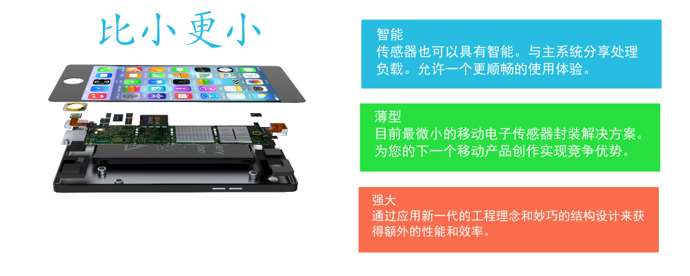
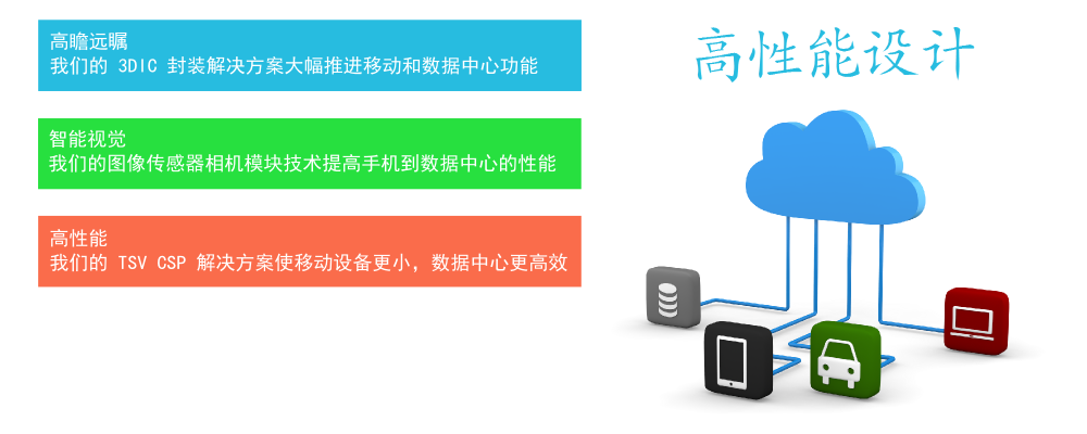
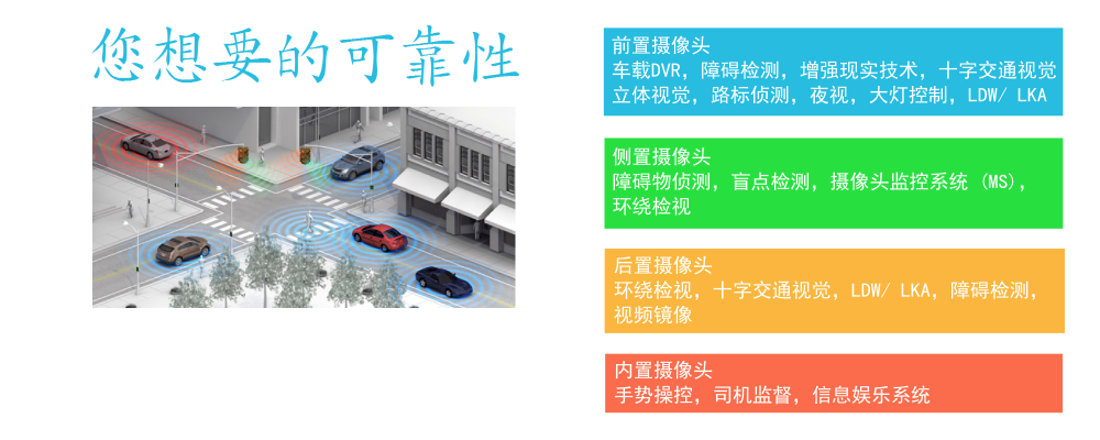
|
|
China Wafer
Level CSP Ltd. is located in Suzhou Industrial Park. It
is a joint venture which
is invested by China-Singapore
Suzhou Industrial Park Ventures
Co . , Ltd. (CSVC) , Infinity - CSVC
Venture Capital Enterprises and Engineering
and IP Advanced Tech Ltd., OmniVision Holding Company Ltd., with a total
capital of 65 million US dollar.
China Wafer Level CSP Ltd enjoys the first ShellOC
technology in the world and is also the sole
company in Mainland China to provide ShellOP, ShellOC
and ShellUT wafer level chip size package services .
After digesting the Shellcase technology from
Israel, China Wafer Level CSP Ltd.
independently developed and owned
several patents for realizing its target goal that the
product is of ‘China Creation’
instead of ‘ China Manufacture’. Those
patents are used in the package process
ideally as the Shellcase technology
does . Up to now , China
Wafer Level CSP Ltd. has passed several
authentications and obtained relevant
certificates.
China Wafer Level CSP Ltd.
currently uses globally advanced
technologies, ShellOC and ShellUT, to package image
sensors mainly. The packaged sensor
chips are greatly highlighted in low weight,
thin height, and small size, and of
high yield derived from the unique packaging process as
the process avoids external
contamination. On the other hand, there is another
advantage associated with wafer level CSP technology,
i.e., smaller is chip size, less is package cost.
The packaged products are widely
applied in camera phones, digital
cameras, fax machine, digital
scanner, CD/DVD portable units, linear sensor, bar code
readers, security, toys and so on. |
|